Journals > > Topics > Optics at Surfaces
Optics at Surfaces|103 Article(s)
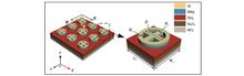
Polarization-Insensitive Highly Selective Color Filter
Gongli Xiao, Miao Li, Hongyan Yang, Bowen Wang, Jiarong Zhang, Kang Chen, and Xingpeng Liu
ObjectiveColor filters are often made of thin films or dye coatings, but are limited by optical diffraction restrictions, they have low resolution and are sensitive to high temperatures and prolonged ultraviolet (UV) ray exposure. Meanwhile, microstructure-based color filters are more adaptable under application scenarios since they may get the necessary light wavelengths by modifying structural or material factors. Microstructure-based color filters have the advantages of stable performance, tunability, and manufacturability over conventional color filters. Additionally, they are usually made of inorganic or high-temperature durable materials, which have a longer service life with extensive applications in many fields, such as complementary metal oxide semiconductor (CMOS) image sensors, liquid crystal screens, and pixel development.MethodsA top double-layer cross circle and a bottom buffer layer comprise the color filter presented in our study. The metal Al and the hydrogen silsesquioxane (HSQ) polymers make up the double-layer cross circle. The bottom is made up of three dielectric layers: a buffer layer of TiO2, a waveguide layer of Al2O3, and a substrate layer of SiO2. The finite difference time domain (FDTD) method is adopted to conduct a comparative investigation into the transmission spectra and color display patterns of four different structural filters. The effects of the structural period, cross ring diameter, cross width, and polarization angle on the transmission spectra and filtering characteristics are also examined.Results and DiscussionsCompared to single-layer construction, the designed color filter using a double-layer cross circle structure has a greater transmittance and reduced full width at half maximum (FWHM). The filter can achieve high transmittance of up to 90.5% at vertical incidence [Fig. 5(b)] and the minimum FWHM at the structural period is L1=W1=360 nm [Fig. 1(a)]. Meanwhile, the resonance wavelength of the transmission peak remains essentially constant over the polarization range of 0-90° (Fig. 5), and the transmittance remains above 50 when the angle of incidence is varied from 0 to 30° (Fig. 6).ConclusionsWe propose a polarization-insensitive and highly selective color filter. FDTD numerical simulation is adopted to investigate and compare the cross ring double-layer subsurface structure to the single-layer plasmonic structure. The results show that combining the double-layer subsurface structure with the dielectric can result in a higher transmittance and narrower FWHM, thus leading to a more effective color selection in the visible wavelength range and robust interference resistance. When the angle of the polarized light is changed from 0 to 90°, the resonance peak position of the simulated transmission spectrum varies somewhat, and the accompanying chromaticity coordinate point moves within a small range. This means that the output properties of the filter are consistent across polarization angles, allowing the filter to be employed in structural applications. ObjectiveColor filters are often made of thin films or dye coatings, but are limited by optical diffraction restrictions, they have low resolution and are sensitive to high temperatures and prolonged ultraviolet (UV) ray exposure. Meanwhile, microstructure-based color filters are more adaptable under application scenarios since they may get the necessary light wavelengths by modifying structural or material factors. Microstructure-based color filters have the advantages of stable performance, tunability, and manufacturability over conventional color filters. Additionally, they are usually made of inorganic or high-temperature durable materials, which have a longer service life with extensive applications in many fields, such as complementary metal oxide semiconductor (CMOS) image sensors, liquid crystal screens, and pixel development.MethodsA top double-layer cross circle and a bottom buffer layer comprise the color filter presented in our study. The metal Al and the hydrogen silsesquioxane (HSQ) polymers make up the double-layer cross circle. The bottom is made up of three dielectric layers: a buffer layer of TiO2, a waveguide layer of Al2O3, and a substrate layer of SiO2. The finite difference time domain (FDTD) method is adopted to conduct a comparative investigation into the transmission spectra and color display patterns of four different structural filters. The effects of the structural period, cross ring diameter, cross width, and polarization angle on the transmission spectra and filtering characteristics are also examined.Results and DiscussionsCompared to single-layer construction, the designed color filter using a double-layer cross circle structure has a greater transmittance and reduced full width at half maximum (FWHM). The filter can achieve high transmittance of up to 90.5% at vertical incidence [Fig. 5(b)] and the minimum FWHM at the structural period is L1=W1=360 nm [Fig. 1(a)]. Meanwhile, the resonance wavelength of the transmission peak remains essentially constant over the polarization range of 0-90° (Fig. 5), and the transmittance remains above 50 when the angle of incidence is varied from 0 to 30° (Fig. 6).ConclusionsWe propose a polarization-insensitive and highly selective color filter. FDTD numerical simulation is adopted to investigate and compare the cross ring double-layer subsurface structure to the single-layer plasmonic structure. The results show that combining the double-layer subsurface structure with the dielectric can result in a higher transmittance and narrower FWHM, thus leading to a more effective color selection in the visible wavelength range and robust interference resistance. When the angle of the polarized light is changed from 0 to 90°, the resonance peak position of the simulated transmission spectrum varies somewhat, and the accompanying chromaticity coordinate point moves within a small range. This means that the output properties of the filter are consistent across polarization angles, allowing the filter to be employed in structural applications.
Acta Optica Sinica
- Publication Date: Apr. 25, 2024
- Vol. 44, Issue 8, 0824001 (2024)

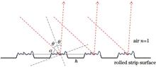
Roll Laser Texturing Technology Based on Uniformly Randomly Distributed Offset Phase
Renhao Ma, Xuanyi Yu, Jianyao Li, Chongyang Shen, and Xiaoxu Deng
ObjectiveCold rolled strips are widely employed in automobiles, home appliances and other industries, and their surface micromorphology affects the surface chromatic aberration of the strip steel. The strip steel surface with regularly distributed microstructure tends to exhibit alternative bright and dark fringes. When the microstructure is randomly distributed, the stripes caused by multi-beam interference will be weakened. The surface microstructure of the rolled strip corresponds to that of the roll surface. The disordered roll laser texturing technology features less pollution, a wide range of texturing roughness, and high surface hardness, which can reduce the surface chromatic aberration of the rolled strip and is expected to meet the growing demand for sound stamping performance and fine brightness after the painting of cold rolled sheet productions.MethodsThe laser texturing roller technology is presented for controlling the range of peak per inch (PPI) density and roughness of rolling rolls based on the offset phase difference of the random distribution. The formation mechanism of light and dark alternately stripes on the surface of rolled strip steel is analyzed using the multi-beam interference principle. By the ray tracing method, the random distribution phase difference generated by the offset of equally spaced convex microstructures is studied to weaken the interference fringes formed by single-wavelength reflected light on the surface of rolled strip steel, which thus eliminates Moiré fringes generated by multiple wavelengths. The reflected coherent irradiance is adopted to study the corresponding uniform distribution function characteristic parameters under different center spacing when the interference fringes are broken. Meanwhile, laser impact pit experiments are conducted on roll material samples to obtain the corresponding relationship between the textured pit morphology and laser impact conditions. The random deviation of the pit microstructure on the roll surface is the same as that of the convex microstructure on the rolling strip by attenuating“copying”. We utilize Matlab's pseudo-random number generator based on the linear congruence method to generate two sets of random arrays that obey the uniform distribution obtained from the simulation analysis. Disordered texturing is performed on the rolling roll material sample by laser impact, which is achieved by adopting deviation in the convex microstructure center distance following a uniform distribution by theoretical and simulation analysis.Results and DiscussionsWhen the center offset of the microstructure on the surface of the rolled strip steel obeys a uniform distribution function, the coherent irradiance disorder of the single wavelength reflected light of the microstructure is better (Fig. 2). When the interference fringes of the reflected light from the tabular microstructure are broken, different center spacing corresponds to various characteristic parameters of the uniform distribution function (Fig. 3).ConclusionsBy employing the uniform distribution function of pit center offset obtained from theoretical and simulation analysis, and the relationship between experimentally obtained laser parameters and pit morphology, the surface of a roll material sample with a roughness of 3.79 μm and PPI of 179 is experimentally realized as disordered laser texturing of the roll material sample in a small area of 10 mm×10 mm by laser texturing technology (Fig. 5). ObjectiveCold rolled strips are widely employed in automobiles, home appliances and other industries, and their surface micromorphology affects the surface chromatic aberration of the strip steel. The strip steel surface with regularly distributed microstructure tends to exhibit alternative bright and dark fringes. When the microstructure is randomly distributed, the stripes caused by multi-beam interference will be weakened. The surface microstructure of the rolled strip corresponds to that of the roll surface. The disordered roll laser texturing technology features less pollution, a wide range of texturing roughness, and high surface hardness, which can reduce the surface chromatic aberration of the rolled strip and is expected to meet the growing demand for sound stamping performance and fine brightness after the painting of cold rolled sheet productions.MethodsThe laser texturing roller technology is presented for controlling the range of peak per inch (PPI) density and roughness of rolling rolls based on the offset phase difference of the random distribution. The formation mechanism of light and dark alternately stripes on the surface of rolled strip steel is analyzed using the multi-beam interference principle. By the ray tracing method, the random distribution phase difference generated by the offset of equally spaced convex microstructures is studied to weaken the interference fringes formed by single-wavelength reflected light on the surface of rolled strip steel, which thus eliminates Moiré fringes generated by multiple wavelengths. The reflected coherent irradiance is adopted to study the corresponding uniform distribution function characteristic parameters under different center spacing when the interference fringes are broken. Meanwhile, laser impact pit experiments are conducted on roll material samples to obtain the corresponding relationship between the textured pit morphology and laser impact conditions. The random deviation of the pit microstructure on the roll surface is the same as that of the convex microstructure on the rolling strip by attenuating“copying”. We utilize Matlab's pseudo-random number generator based on the linear congruence method to generate two sets of random arrays that obey the uniform distribution obtained from the simulation analysis. Disordered texturing is performed on the rolling roll material sample by laser impact, which is achieved by adopting deviation in the convex microstructure center distance following a uniform distribution by theoretical and simulation analysis.Results and DiscussionsWhen the center offset of the microstructure on the surface of the rolled strip steel obeys a uniform distribution function, the coherent irradiance disorder of the single wavelength reflected light of the microstructure is better (Fig. 2). When the interference fringes of the reflected light from the tabular microstructure are broken, different center spacing corresponds to various characteristic parameters of the uniform distribution function (Fig. 3).ConclusionsBy employing the uniform distribution function of pit center offset obtained from theoretical and simulation analysis, and the relationship between experimentally obtained laser parameters and pit morphology, the surface of a roll material sample with a roughness of 3.79 μm and PPI of 179 is experimentally realized as disordered laser texturing of the roll material sample in a small area of 10 mm×10 mm by laser texturing technology (Fig. 5).
Acta Optica Sinica
- Publication Date: Mar. 10, 2024
- Vol. 44, Issue 5, 0524001 (2024)
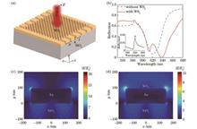
Strong Coupling Between Surface Plasmons in Metallic Grating and Excitons in Tungsten Disulfide
Yingwen Su, Hua Lu, Shouhao Shi, Dikun Li, Xiangxian Wang, and Jianlin Zhao
ObjectiveIn recent years, strong coupling between surface plasmons and excitons has become a research hotspot in light-matter interactions. As an important two-dimensional material, transition metal dichalcogenides (TMDs) have caught extensive attention due to their unique optoelectrical properties. TMD monolayers are direct band gap semiconductors and their excitons have large transition dipole moments and binding energy, which is beneficial to realize the strong coupling between photons and excitons at room temperature. Surface plasmons in metallic nanostructures feature near-field enhancement and small mode volume, providing an effective platform for realizing its strong coupling with excitons. Recently, the strong coupling has been achieved between surface plasmons and TMD excitons in plasmonic systems such as metallic nanoarray, nanoparticles, and nanocavities. One-dimensional (1D) metallic grating is a typical plasmonic structure, in which the coupling effect between surface plasmons and TMD excitons has been rarely studied till now. Thus, we investigate the plasmon-exciton strong coupling behavior in the 1D metallic grating integrated with monolayer tungsten disulfide (WS2).MethodWe build a simulation model by adopting the finite-difference time-domain (FDTD) method and numerically investigate the coupling effect between surface plasmons in the gold grating and excitons in monolayer WS2. The dielectric constants of gold and monolayer WS2 are described by the Drude model and high-order Lorentz model respectively. The spectral response and electric field distribution of the gold grating structure and gold grating/monolayer WS2 hybrid structure are calculated. We study the dependence of reflection spectra on the structural parameters (grating pitch p, width l, and height h) in the gold grating and gold grating/monolayer WS2 hybrid structures. Based on the temporal coupled-mode theory, we build a model of optical coupling between surface plasmons in the gold grating and excitons in monolayer WS2 and thus derive the theoretical formula of the reflection spectrum from the hybrid structure. The temporal coupled-mode theory is employed to fit the reflection spectra of the hybrid structures. Thus, we obtain the fitting parameters containing plasmonic and exciton decay rates and coupling strength in the hybrid structures with different grating heights. Then, the coupled oscillator model is utilized to calculate the splitting energy of the reflection spectra from the gold grating/monolayer WS2 hybrid structures. Finally, the dependence of the reflection spectrum on the environmental refractive index is studied by FDTD simulation.Results and DiscussionsThe results show that the reflection spectrum of the gold grating with the pitch p = 400 nm, width l = 300 nm, and height h = 95 nm possesses an obvious dip at the wavelength of 620 nm due to the generation of surface plasmons. When the monolayer WS2 is integrated with the gold grating, the plasmonic reflection spectrum will be split. There is an obvious reflection peak at 620 nm wavelength in the original reflection dip with two reflection dips around the peak [Fig. 1(b)]. The electric field of the gold grating is mainly localized at the vertex of the gold grating. With a monolayer WS2, the electric field intensity is weakened [Figs. 1(c) and 1(d)]. With the increasing pitch, width, and height, the reflection dip of the gold grating has a red-shifted [Figs. 2(a), 3(a), and 4(a)]. The reflection spectra of the hybrid structure are fitted by the temporal coupled-mode theory, and they are in good agreement with the simulated spectra [Figs. 2(b), 3(b), and 4(b)]. We find that the fitted decay rate and coupling strength are not sensitive to the height of the gold grating, and the plasmonic resonance frequency decreases with increasing h (Fig. 5). The analyzed results yielded by the coupled oscillator model show that the coupling between the surface plasmons and the excitons in the hybrid structure satisfies the criterion of strong coupling with the Rabi splitting of 54.6 meV (Fig. 6). The relationship between the coupling spectrum and environmental refractive index is studied in the hybrid structure. The wavelength difference between the two reflection dips is found to be approximately linear with the refractive index, which provides a possible way for optical sensing (Fig. 7).ConclusionsThe coupling characteristics of surface plasmons in the gold grating and excitons in monolayer WS2 are studied. The spectral response and electric field distribution of the 1D gold grating/monolayer WS2 hybrid structure are simulated by the FDTD simulation. The results show that the coupling between surface plasmons in the gold grating and excitons in monolayer WS2 can generate spectral splitting. The reflection spectra of the hybrid structure with different structural parameters are fitted by adopting the temporal coupled-mode theory. The fitting results are in good agreement with the numerical simulation. The theoretical analysis shows that the coupling between surface plasmons in the gold grating and excitons in the monolayer WS2 satisfies the strong coupling criterion. The Rabi splitting of coupling spectra from the hybrid structure is 54.6 meV, which is consistent with the temporal coupled-mode theoretical result. The simulation results show that the wavelength difference between the spectral dips of strong coupling presents nearly linear relations with the environmental refractive index, which will offer a new way for optical sensing. Additionally, this work will provide a new method for plasmon-exciton strong coupling in metallic grating integrated with TMDs and its applications in optical devices. ObjectiveIn recent years, strong coupling between surface plasmons and excitons has become a research hotspot in light-matter interactions. As an important two-dimensional material, transition metal dichalcogenides (TMDs) have caught extensive attention due to their unique optoelectrical properties. TMD monolayers are direct band gap semiconductors and their excitons have large transition dipole moments and binding energy, which is beneficial to realize the strong coupling between photons and excitons at room temperature. Surface plasmons in metallic nanostructures feature near-field enhancement and small mode volume, providing an effective platform for realizing its strong coupling with excitons. Recently, the strong coupling has been achieved between surface plasmons and TMD excitons in plasmonic systems such as metallic nanoarray, nanoparticles, and nanocavities. One-dimensional (1D) metallic grating is a typical plasmonic structure, in which the coupling effect between surface plasmons and TMD excitons has been rarely studied till now. Thus, we investigate the plasmon-exciton strong coupling behavior in the 1D metallic grating integrated with monolayer tungsten disulfide (WS2).MethodWe build a simulation model by adopting the finite-difference time-domain (FDTD) method and numerically investigate the coupling effect between surface plasmons in the gold grating and excitons in monolayer WS2. The dielectric constants of gold and monolayer WS2 are described by the Drude model and high-order Lorentz model respectively. The spectral response and electric field distribution of the gold grating structure and gold grating/monolayer WS2 hybrid structure are calculated. We study the dependence of reflection spectra on the structural parameters (grating pitch p, width l, and height h) in the gold grating and gold grating/monolayer WS2 hybrid structures. Based on the temporal coupled-mode theory, we build a model of optical coupling between surface plasmons in the gold grating and excitons in monolayer WS2 and thus derive the theoretical formula of the reflection spectrum from the hybrid structure. The temporal coupled-mode theory is employed to fit the reflection spectra of the hybrid structures. Thus, we obtain the fitting parameters containing plasmonic and exciton decay rates and coupling strength in the hybrid structures with different grating heights. Then, the coupled oscillator model is utilized to calculate the splitting energy of the reflection spectra from the gold grating/monolayer WS2 hybrid structures. Finally, the dependence of the reflection spectrum on the environmental refractive index is studied by FDTD simulation.Results and DiscussionsThe results show that the reflection spectrum of the gold grating with the pitch p = 400 nm, width l = 300 nm, and height h = 95 nm possesses an obvious dip at the wavelength of 620 nm due to the generation of surface plasmons. When the monolayer WS2 is integrated with the gold grating, the plasmonic reflection spectrum will be split. There is an obvious reflection peak at 620 nm wavelength in the original reflection dip with two reflection dips around the peak [Fig. 1(b)]. The electric field of the gold grating is mainly localized at the vertex of the gold grating. With a monolayer WS2, the electric field intensity is weakened [Figs. 1(c) and 1(d)]. With the increasing pitch, width, and height, the reflection dip of the gold grating has a red-shifted [Figs. 2(a), 3(a), and 4(a)]. The reflection spectra of the hybrid structure are fitted by the temporal coupled-mode theory, and they are in good agreement with the simulated spectra [Figs. 2(b), 3(b), and 4(b)]. We find that the fitted decay rate and coupling strength are not sensitive to the height of the gold grating, and the plasmonic resonance frequency decreases with increasing h (Fig. 5). The analyzed results yielded by the coupled oscillator model show that the coupling between the surface plasmons and the excitons in the hybrid structure satisfies the criterion of strong coupling with the Rabi splitting of 54.6 meV (Fig. 6). The relationship between the coupling spectrum and environmental refractive index is studied in the hybrid structure. The wavelength difference between the two reflection dips is found to be approximately linear with the refractive index, which provides a possible way for optical sensing (Fig. 7).ConclusionsThe coupling characteristics of surface plasmons in the gold grating and excitons in monolayer WS2 are studied. The spectral response and electric field distribution of the 1D gold grating/monolayer WS2 hybrid structure are simulated by the FDTD simulation. The results show that the coupling between surface plasmons in the gold grating and excitons in monolayer WS2 can generate spectral splitting. The reflection spectra of the hybrid structure with different structural parameters are fitted by adopting the temporal coupled-mode theory. The fitting results are in good agreement with the numerical simulation. The theoretical analysis shows that the coupling between surface plasmons in the gold grating and excitons in the monolayer WS2 satisfies the strong coupling criterion. The Rabi splitting of coupling spectra from the hybrid structure is 54.6 meV, which is consistent with the temporal coupled-mode theoretical result. The simulation results show that the wavelength difference between the spectral dips of strong coupling presents nearly linear relations with the environmental refractive index, which will offer a new way for optical sensing. Additionally, this work will provide a new method for plasmon-exciton strong coupling in metallic grating integrated with TMDs and its applications in optical devices.
Acta Optica Sinica
- Publication Date: Feb. 25, 2024
- Vol. 44, Issue 4, 0424002 (2024)
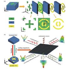
Multi-Frequency and Multi-Beam Tunable Terahertz Coding Metasurface in Full Space
Zhixiong Yang, Jingli Wang, Wenjun Sun, Liang Yin, Xianchao Dong, Hongdan Wan, Heming Chen, and Kai Zhong
ObjectiveTerahertz waves refer to electromagnetic waves between microwave and infrared wave, which can be applied in different fields such as communication, sensing, radar, and imaging. Terahertz coding metasurface, as an important device for modulating terahertz waves, has the advantages of simple structure, small size, low cost, low loss, and high efficiency. The coding metasurface units are arranged according to a certain coding sequence, and by changing the phase difference between the units, the flexible modulation of terahertz waves can be achieved to generate various forms of beams. However, when the design of a general terahertz coding metasurface is completed, the function and operating frequency are relatively single. In order to fully utilize the coding metasurface, an anisotropic metasurface is proposed, which can regulate the incident orthogonal polarized waves separately. And a frequency independent coding metasurface has been proposed, which can separately regulate the incidence waves at different frequency points to generate different forms of beams. In addition, the phase change materials such as vanadium dioxide (VO2) were used to achieve the switching of transmission and reflection modes of terahertz waves, thereby achieving the goal of full spatial modulation of electromagnetic waves. The above methods improve the ability of the coding metasurface to regulate terahertz waves, but the integration level still needs to be improved. Therefore, we integrate these technologies to achieve multi-frequency and multi-beam tunable terahertz coding metasurface in full space, greatly improving its ability to regulate terahertz waves.MethodsIn this paper, a coding metasurface which can regulate the circular polarized waves and orthogonal polarized waves separately is proposed by combining the principle of PB geometrical phase as well as the frequency independence and anisotropy of double crosses. In addition, introducing the phase change material VO2, flexible switching of terahertz waves between transmission and reflection is achieved by changing its phase change state. The details are as follows. When VO2 is in an insulating state, the designed coding metasurface is a single-frequency-point 3-bit PB geometrical phase transmitting coding metasurface, which generates transmission-type vortex waves with topological charge number of 1. When VO2 is in a metallic state, the designed coding metasurface is a dual-frequency-point independently adjustable 1-bit anisotropic reflective coding metasurface, which generates four symmetric beams, of which two symmetric beams on the xoz plane with RCS reduction and two symmetric beams are on the yoz plane, respectively.Results and DiscussionsThe designed coding metasurface units (Fig. 1) with identical metallic split-ring structures in the third, fifth, and seventh layers are rotated from 0° to 157.5° in a step of 22.5° to obtain a total of eight coding metasurface units (Fig. 2). When VO2 is in an insulating state and a circularly polarized wave with f1=0.6 THz is incident, the units maintain a high transmission amplitude and strictly satisfy a phase difference of 45°. The design conditions for a 3-bit transmission type coding metasurface unit are met. Arranging them according to a certain coding sequence [Fig.4(b)] can produce transmission-type vortex waves with topological charge number of 1 (Fig.5). When VO2 is in a metallic state and the orthogonal polarized waves of f2=0.5 THz and f3=0.85 THz are incident, a dual-frequency and anisotropic 1-bit reflective-type coding metasurface unit (Fig. 3) is designed by using the two cross structures. After arranging them according to a certain coding sequence [Figs. 4 (c)-(f)], the perpendicular incidence of y-polarized wave with f2=0.5 THz on the xoz plane produces two symmetric beams [Figs. 6(a) and 6(b)]. When a y-polarized wave with f3=0.85 THz is incident vertically, two symmetric beams are generated on the yoz plane [Figs. 6(c) and 6(d)]. When a x-polarized wave with f2=0.5 THz is incident vertically, four symmetrical beams are generated [Figs. 7(a) and 7(b)]. When a x-polarized wave with f3=0.85 THz is incident vertically, a diffuse scattering beam can be generated [Figs. 8(a) and 8(b)], realizing RCS reduction. The results show that with the rational design of the coding metasurface combined with the phase transition state of VO2, the frequency of the incident wave source, and the polarization state, the full space regulation of terahertz wave's reflection and transmission can be realized and five beam forms on the same coding metasurface can be obtained.ConclusionsIn this paper, a coding metasurface with full space multi-frequency and multi-beam tunability is designed by changing the phase transition state of VO2, combining the principle of PB geometrical phase and the cross unit structure with dual-frequency anisotropy. A 3-bit transmission coding metasurface with an operating frequency of f1=0.6 THz is designed to produce a transmitted vortex beam. And a dual-frequency 1-bit anisotropic reflective coding metasurface with operating frequencies of f2=0.5 THz and f3=0.85 THz is designed to produce various forms of symmetric and scattered beams. This coding metasurface, which introduces phase change material and realizes full space multi-frequency multi-beam regulation by transmission and reflection, is important for designing multifunctional terahertz beam modulation devices. ObjectiveTerahertz waves refer to electromagnetic waves between microwave and infrared wave, which can be applied in different fields such as communication, sensing, radar, and imaging. Terahertz coding metasurface, as an important device for modulating terahertz waves, has the advantages of simple structure, small size, low cost, low loss, and high efficiency. The coding metasurface units are arranged according to a certain coding sequence, and by changing the phase difference between the units, the flexible modulation of terahertz waves can be achieved to generate various forms of beams. However, when the design of a general terahertz coding metasurface is completed, the function and operating frequency are relatively single. In order to fully utilize the coding metasurface, an anisotropic metasurface is proposed, which can regulate the incident orthogonal polarized waves separately. And a frequency independent coding metasurface has been proposed, which can separately regulate the incidence waves at different frequency points to generate different forms of beams. In addition, the phase change materials such as vanadium dioxide (VO2) were used to achieve the switching of transmission and reflection modes of terahertz waves, thereby achieving the goal of full spatial modulation of electromagnetic waves. The above methods improve the ability of the coding metasurface to regulate terahertz waves, but the integration level still needs to be improved. Therefore, we integrate these technologies to achieve multi-frequency and multi-beam tunable terahertz coding metasurface in full space, greatly improving its ability to regulate terahertz waves.MethodsIn this paper, a coding metasurface which can regulate the circular polarized waves and orthogonal polarized waves separately is proposed by combining the principle of PB geometrical phase as well as the frequency independence and anisotropy of double crosses. In addition, introducing the phase change material VO2, flexible switching of terahertz waves between transmission and reflection is achieved by changing its phase change state. The details are as follows. When VO2 is in an insulating state, the designed coding metasurface is a single-frequency-point 3-bit PB geometrical phase transmitting coding metasurface, which generates transmission-type vortex waves with topological charge number of 1. When VO2 is in a metallic state, the designed coding metasurface is a dual-frequency-point independently adjustable 1-bit anisotropic reflective coding metasurface, which generates four symmetric beams, of which two symmetric beams on the xoz plane with RCS reduction and two symmetric beams are on the yoz plane, respectively.Results and DiscussionsThe designed coding metasurface units (Fig. 1) with identical metallic split-ring structures in the third, fifth, and seventh layers are rotated from 0° to 157.5° in a step of 22.5° to obtain a total of eight coding metasurface units (Fig. 2). When VO2 is in an insulating state and a circularly polarized wave with f1=0.6 THz is incident, the units maintain a high transmission amplitude and strictly satisfy a phase difference of 45°. The design conditions for a 3-bit transmission type coding metasurface unit are met. Arranging them according to a certain coding sequence [Fig.4(b)] can produce transmission-type vortex waves with topological charge number of 1 (Fig.5). When VO2 is in a metallic state and the orthogonal polarized waves of f2=0.5 THz and f3=0.85 THz are incident, a dual-frequency and anisotropic 1-bit reflective-type coding metasurface unit (Fig. 3) is designed by using the two cross structures. After arranging them according to a certain coding sequence [Figs. 4 (c)-(f)], the perpendicular incidence of y-polarized wave with f2=0.5 THz on the xoz plane produces two symmetric beams [Figs. 6(a) and 6(b)]. When a y-polarized wave with f3=0.85 THz is incident vertically, two symmetric beams are generated on the yoz plane [Figs. 6(c) and 6(d)]. When a x-polarized wave with f2=0.5 THz is incident vertically, four symmetrical beams are generated [Figs. 7(a) and 7(b)]. When a x-polarized wave with f3=0.85 THz is incident vertically, a diffuse scattering beam can be generated [Figs. 8(a) and 8(b)], realizing RCS reduction. The results show that with the rational design of the coding metasurface combined with the phase transition state of VO2, the frequency of the incident wave source, and the polarization state, the full space regulation of terahertz wave's reflection and transmission can be realized and five beam forms on the same coding metasurface can be obtained.ConclusionsIn this paper, a coding metasurface with full space multi-frequency and multi-beam tunability is designed by changing the phase transition state of VO2, combining the principle of PB geometrical phase and the cross unit structure with dual-frequency anisotropy. A 3-bit transmission coding metasurface with an operating frequency of f1=0.6 THz is designed to produce a transmitted vortex beam. And a dual-frequency 1-bit anisotropic reflective coding metasurface with operating frequencies of f2=0.5 THz and f3=0.85 THz is designed to produce various forms of symmetric and scattered beams. This coding metasurface, which introduces phase change material and realizes full space multi-frequency multi-beam regulation by transmission and reflection, is important for designing multifunctional terahertz beam modulation devices.
Acta Optica Sinica
- Publication Date: Feb. 25, 2024
- Vol. 44, Issue 4, 0424001 (2024)
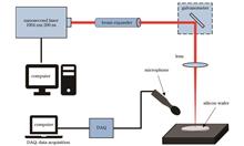
Acoustic Signal Monitoring in Laser Ablation of Anti-Reflective Microstructured Silicon Surface
Weipeng Huang, Rui Zhou, Zhekun Chen, Gongfa Yuan, and Qile Liao
ObjectiveAnti-reflective microstructured silicon surface could greatly improve the light trapping performance for silicon-based energy harvesting devices, thereby increasing the optical absorption efficiency and reducing the surface reflection. In the manufacturing of anti-reflective silicon surfaces, the thermal effect produced by laser ablation may lead to the collapse of microstructures with high aspect ratios, thus resulting in the rapid increase of reflectivity by seriously affecting the light trapping effect on microstructured silicon surfaces. Therefore, the microstructure characterization on silicon surfaces is of great significance for product quality and loss assessment of parts. Currently, offline methods including spectrometer or scanning electron microscopy (SEM) are widely employed. It needs to transfer the samples for observation after the preparation, and the fabricating process could not be optimized in time referring to processing results. To improve the quality of laser processing on anti-reflective silicon surfaces and shorten the optimization periods, researchers have proposed corresponding solutions via real-time monitoring. Laser ablation is often accompanied by the generation of acoustic, optical, electrical and thermal signals, and can be monitored based on a variety of sensors in real-time. Compared with other signals, acoustic signals exhibit excellent spatial resolution. At present, real-time monitoring technology based on acoustic signals is mostly adopted to monitor the changes in laser parameters or processing quality, while few studies focus on the forming of surface microstructures. Therefore, a real-time acoustic signal monitoring and processing method is put forward based on time-frequency domain processing to analyze the forming process of surface microstructures.MethodsIn this paper, real-time monitoring of acoustic signals includes two steps of sampling and feature extraction. The acoustic signal is converted into electrical signal through a pre-polarized capacitive microphone with a frequency response range from 20 Hz to 31.5 kHz. Then, the electrical signal is collected by an oscilloscope at a sampling frequency of 240 kHz. The frequency composition of real-time signal and its intensity change with time could be obtained by MATLAB software for short-time Fourier transform and fast Fourier transform. The acoustic signal is normalized in the characteristic section, and the proportion of the amplitude in the frequency domain of the acoustic signal could be extracted as the characteristic parameter for analysis to improve the linearity between the characteristic parameters of the acoustic signal and the average depth of surface microstructures. Based on the sound source generation mechanism, the surface morphology of the silicon surface during laser ablation could be monitored by the time-frequency spectrum of the corresponding acoustic signal. An acoustic measurement method based on the fast Fourier transform is proposed to obtain the height and width of microstructures. The reflectivity of the sample is considered the evaluation standard of the sample processing quality, and the amplitude of each acoustic signal frequency is taken as the input. The artificial neural network is applied to predict the processing quality of the anti-reflective silicon surface.Results and DiscussionsFirstly, the correlation between the acoustic signals in 0-30 kHz and characteristic sizes of the surface microstructure fabricated by laser ablation could be analyzed by the time-frequency spectrum of the acoustic signal. The acoustic signal generated during laser processing can reflect whether the ablated silicon surface forms periodic microstructure (Fig. 3), and the frequency composition of the acoustic signal could be tuned by microstructured width (Fig. 4). Then the effects of laser power and processing times on the microstructure depth are analyzed in detail, corresponding to the amplitude changes of each acoustic signal frequency. In the case of a fixed microstructure width, the normalized acoustic signal characteristic parameters change linearly with the microstructured depth, and the influence of laser power changes could be ignored (Fig. 10). Additionally, an artificial neural network is applied to forecast the processing quality by utilizing the acoustic signal as the input. The reflectivity of 5% on the silicon surface is defined as the processing quality boundary, and the actual measurement accuracy of processing quality prediction could exceed 90% via the artificial neural network. This indicates that the acoustic online monitoring can be employed to evaluate the surface processing quality of anti-reflective silicon surface in real-time (Fig. 13).ConclusionsThe real-time acoustic signal analysis in this paper can effectively monitor the surface microstructure morphology and predict the machining quality. Results show that the acoustic signal with the same frequency could be always captured during laser processing, regardless of whether the microstructured surface exists or not. The acoustic signal frequency related to the microstructure could be influenced by the microstructure depth and laser scanning speed. The ratio of the frequency component intensity to the total signal intensity is linearly correlated to the average structural depth on microstructured silicon surfaces. The proposed method can effectively work even after partial structured collapse. The artificial neural network is adopted to verify the correlation between the acoustic signal and the machining quality. The accuracy of the classification prediction is higher than 90%. This study provides a theoretical basis for the real-time quality monitoring of anti-reflective silicon surfaces fabricated by laser ablation. In the future, more attention could be paid to the underlying mechanism and monitoring method of acoustic signal generation at the moment of microstructured collapse, which could be combined with other existing signal processing methods to yield better processing quality. ObjectiveAnti-reflective microstructured silicon surface could greatly improve the light trapping performance for silicon-based energy harvesting devices, thereby increasing the optical absorption efficiency and reducing the surface reflection. In the manufacturing of anti-reflective silicon surfaces, the thermal effect produced by laser ablation may lead to the collapse of microstructures with high aspect ratios, thus resulting in the rapid increase of reflectivity by seriously affecting the light trapping effect on microstructured silicon surfaces. Therefore, the microstructure characterization on silicon surfaces is of great significance for product quality and loss assessment of parts. Currently, offline methods including spectrometer or scanning electron microscopy (SEM) are widely employed. It needs to transfer the samples for observation after the preparation, and the fabricating process could not be optimized in time referring to processing results. To improve the quality of laser processing on anti-reflective silicon surfaces and shorten the optimization periods, researchers have proposed corresponding solutions via real-time monitoring. Laser ablation is often accompanied by the generation of acoustic, optical, electrical and thermal signals, and can be monitored based on a variety of sensors in real-time. Compared with other signals, acoustic signals exhibit excellent spatial resolution. At present, real-time monitoring technology based on acoustic signals is mostly adopted to monitor the changes in laser parameters or processing quality, while few studies focus on the forming of surface microstructures. Therefore, a real-time acoustic signal monitoring and processing method is put forward based on time-frequency domain processing to analyze the forming process of surface microstructures.MethodsIn this paper, real-time monitoring of acoustic signals includes two steps of sampling and feature extraction. The acoustic signal is converted into electrical signal through a pre-polarized capacitive microphone with a frequency response range from 20 Hz to 31.5 kHz. Then, the electrical signal is collected by an oscilloscope at a sampling frequency of 240 kHz. The frequency composition of real-time signal and its intensity change with time could be obtained by MATLAB software for short-time Fourier transform and fast Fourier transform. The acoustic signal is normalized in the characteristic section, and the proportion of the amplitude in the frequency domain of the acoustic signal could be extracted as the characteristic parameter for analysis to improve the linearity between the characteristic parameters of the acoustic signal and the average depth of surface microstructures. Based on the sound source generation mechanism, the surface morphology of the silicon surface during laser ablation could be monitored by the time-frequency spectrum of the corresponding acoustic signal. An acoustic measurement method based on the fast Fourier transform is proposed to obtain the height and width of microstructures. The reflectivity of the sample is considered the evaluation standard of the sample processing quality, and the amplitude of each acoustic signal frequency is taken as the input. The artificial neural network is applied to predict the processing quality of the anti-reflective silicon surface.Results and DiscussionsFirstly, the correlation between the acoustic signals in 0-30 kHz and characteristic sizes of the surface microstructure fabricated by laser ablation could be analyzed by the time-frequency spectrum of the acoustic signal. The acoustic signal generated during laser processing can reflect whether the ablated silicon surface forms periodic microstructure (Fig. 3), and the frequency composition of the acoustic signal could be tuned by microstructured width (Fig. 4). Then the effects of laser power and processing times on the microstructure depth are analyzed in detail, corresponding to the amplitude changes of each acoustic signal frequency. In the case of a fixed microstructure width, the normalized acoustic signal characteristic parameters change linearly with the microstructured depth, and the influence of laser power changes could be ignored (Fig. 10). Additionally, an artificial neural network is applied to forecast the processing quality by utilizing the acoustic signal as the input. The reflectivity of 5% on the silicon surface is defined as the processing quality boundary, and the actual measurement accuracy of processing quality prediction could exceed 90% via the artificial neural network. This indicates that the acoustic online monitoring can be employed to evaluate the surface processing quality of anti-reflective silicon surface in real-time (Fig. 13).ConclusionsThe real-time acoustic signal analysis in this paper can effectively monitor the surface microstructure morphology and predict the machining quality. Results show that the acoustic signal with the same frequency could be always captured during laser processing, regardless of whether the microstructured surface exists or not. The acoustic signal frequency related to the microstructure could be influenced by the microstructure depth and laser scanning speed. The ratio of the frequency component intensity to the total signal intensity is linearly correlated to the average structural depth on microstructured silicon surfaces. The proposed method can effectively work even after partial structured collapse. The artificial neural network is adopted to verify the correlation between the acoustic signal and the machining quality. The accuracy of the classification prediction is higher than 90%. This study provides a theoretical basis for the real-time quality monitoring of anti-reflective silicon surfaces fabricated by laser ablation. In the future, more attention could be paid to the underlying mechanism and monitoring method of acoustic signal generation at the moment of microstructured collapse, which could be combined with other existing signal processing methods to yield better processing quality.
Acta Optica Sinica
- Publication Date: May. 10, 2023
- Vol. 43, Issue 9, 0924001 (2023)

Application Condition of Effective Medium Theory in Optical Composite System
Yang Sun, and Yongyou Zhang
ObjectiveThe rapid development of micro-nano fabrication technologies enables the synthesis of various optical metamaterials with complex microstructures. The size or component ratio of optical metamaterials can be tuned to control the dielectric properties of optical metamaterials in a wide range. Therefore, analyzing the effective optical parameters of metamaterials has always been a core issue in electromagnetic computing. It is known that the traditional analysis methods for effective optical parameters of composite materials include Maxwell-Garnet effective medium theory and Bruggeman effective medium theory. However, they can only analyze the cases with a small difference between the dielectric constants of the doped and background crystals. When such a difference is large, the error of effective permittivity given by the effective medium theory becomes large as well. This work uses the transfer-matrix method to analyze the effective permittivity of optical metamaterials and discusses the application scope of the effective medium theory.MethodsFor convenience, we assume that the nanocrystals are periodically doped into the background crystal to form a composite system and the nanocrystals and background crystal are isotropic. These allow us to use the transfer-matrix method to calculate the transmission spectrum of the composite system, and then obtain the effective dielectric constant of the composite system by comparing the transmission spectrum of the original structure with that of the equivalent crystal. The matching degree between equivalent transmission spectrum and original transmission spectrum is measured by the coefficient of determination R2. A larger value of R2 means the effective dielectric constant is more accurate.Results and DiscussionsThis work analyzes the dependence of the effective dielectric constant of composite crystals on the dielectric constant of each component, the geometry parameters of composite crystals, and the light wavelength. The comparison of the effective dielectric constants obtained from the transfer-matrix method and the Bruggeman effective medium theory separately indicates that the Bruggeman effective medium theory is indeed only applicable to the case with a small difference between the dielectric constants of the doped and background crystals (Fig. 3). The effective permittivity given by Bruggeman effective medium theory only relates to the volume fraction of nanocrystals and is independent of the light wavelength (Fig. 2 and Fig. 4). However, it is found that the effective dielectric constants rely on the light wavelength after the comparison of the equivalent transmission spectrum and the original transmission spectrum by the transfer-matrix method (Fig. 5). In particular, there is no effective dielectric constant at the optical band gap of the composite system due to the scattering of optical lattices.ConclusionsWhen the difference between the dielectric constants of nanocrystals and background crystal is small, the effective dielectric constant of the composite system is consistent with the result of Bruggeman effective medium theory. However, when the wavelength dependence of the effective dielectric constant is considered, the effective medium theory can be extended to the case with a large difference. This can broaden the application scope of the effective medium theory. It is also found that there is no effective dielectric constant at the optical band gap of the composite system as a homogeneous material has no band gap. These conclusions can provide theoretical guidance for research on the optical properties of composite materials and help determine whether the effective medium theory is applicable. ObjectiveThe rapid development of micro-nano fabrication technologies enables the synthesis of various optical metamaterials with complex microstructures. The size or component ratio of optical metamaterials can be tuned to control the dielectric properties of optical metamaterials in a wide range. Therefore, analyzing the effective optical parameters of metamaterials has always been a core issue in electromagnetic computing. It is known that the traditional analysis methods for effective optical parameters of composite materials include Maxwell-Garnet effective medium theory and Bruggeman effective medium theory. However, they can only analyze the cases with a small difference between the dielectric constants of the doped and background crystals. When such a difference is large, the error of effective permittivity given by the effective medium theory becomes large as well. This work uses the transfer-matrix method to analyze the effective permittivity of optical metamaterials and discusses the application scope of the effective medium theory.MethodsFor convenience, we assume that the nanocrystals are periodically doped into the background crystal to form a composite system and the nanocrystals and background crystal are isotropic. These allow us to use the transfer-matrix method to calculate the transmission spectrum of the composite system, and then obtain the effective dielectric constant of the composite system by comparing the transmission spectrum of the original structure with that of the equivalent crystal. The matching degree between equivalent transmission spectrum and original transmission spectrum is measured by the coefficient of determination R2. A larger value of R2 means the effective dielectric constant is more accurate.Results and DiscussionsThis work analyzes the dependence of the effective dielectric constant of composite crystals on the dielectric constant of each component, the geometry parameters of composite crystals, and the light wavelength. The comparison of the effective dielectric constants obtained from the transfer-matrix method and the Bruggeman effective medium theory separately indicates that the Bruggeman effective medium theory is indeed only applicable to the case with a small difference between the dielectric constants of the doped and background crystals (Fig. 3). The effective permittivity given by Bruggeman effective medium theory only relates to the volume fraction of nanocrystals and is independent of the light wavelength (Fig. 2 and Fig. 4). However, it is found that the effective dielectric constants rely on the light wavelength after the comparison of the equivalent transmission spectrum and the original transmission spectrum by the transfer-matrix method (Fig. 5). In particular, there is no effective dielectric constant at the optical band gap of the composite system due to the scattering of optical lattices.ConclusionsWhen the difference between the dielectric constants of nanocrystals and background crystal is small, the effective dielectric constant of the composite system is consistent with the result of Bruggeman effective medium theory. However, when the wavelength dependence of the effective dielectric constant is considered, the effective medium theory can be extended to the case with a large difference. This can broaden the application scope of the effective medium theory. It is also found that there is no effective dielectric constant at the optical band gap of the composite system as a homogeneous material has no band gap. These conclusions can provide theoretical guidance for research on the optical properties of composite materials and help determine whether the effective medium theory is applicable.
Acta Optica Sinica
- Publication Date: Mar. 10, 2023
- Vol. 43, Issue 5, 0524001 (2023)
Terahertz Dielectric Metasurface for Dual-Dimensional Multi-Channel Multiplexing
Ling Wang, Feng Gao, Shuhua Teng, Zhiguo Tan, Xing Zhang, Jun Lou, and Li Deng
Results and Discussions When the rotation angle φrot of the unit cell is 0°, 30°, 70°, 120°, and 180°, the variations of the simulated phase and normalized amplitude of the cross-polarized transmission coefficient TRL with frequency under LCP incident waves show that the 3 dB bandwidth of TRL of the dielectric unit cell is 0.1 THz, and the working frequency band is about 0.25-0.35 THz (with a relative bandwidth of 33.3%). In addition, as the rotation angle of the unit cell changes from 0° to 180°, the unit cell can cover the phase change of 0°-360° (Fig. 2). Therefore, the metasurface can be realized on the basis of the PB phase principle and the designed dielectric unit cell. When LCP plane waves with the frequency f1 and angle θi(f1) are incident on the metasurface in ±x and ±y directions separately, simulated far-field amplitude and phase patterns of RCP transmission waves show that four-channel beams are generated in the direction perpendicular to the metasurface. At the same time, according to the characteristics of OAM beam energy and phase distribution, the amplitude of one of the transmitted waves is in a solid distribution, with the phase unchanged, and thus, the topological charge l1 equals 0. For the other three-channel beams, the amplitude and phases are distributed in circular and spiral shapes, respectively, and when observed along the -z-axis, the phase changes by +4π, -4π, and +8π in a clockwise direction. In other words, the three-channel OAM beams with topological charges of l2=-2, l3=+2, and l4=-4 are generated. It can be seen that four-channel topologically orthogonal coaxial beams with frequency f1 are generated in the direction perpendicular to the metasurface (Fig. 5). Similarly, for four-channel LCP plane waves with f2 and θi(f1), or f3 and θi(f3) incident on the metasurface along the ±x and ±y axes, four topologically orthogonal coaxial beams with frequency f2 or f3 in the direction perpendicular to the metasurface are generated (Figs. 6 and 7).ObjectiveIn recent years, the terahertz (THz) band has attracted extensive attention from researchers due to its potential of realizing high-speed and high-capacity wireless communication systems. The multiplexing technology has great research prospects in improving the communication rate and system capacity. The electromagnetic wave (EMW) carrying the orbital angular momentum (OAM) is called the OAM wave. OAM can be used as a new information carrier to provide an additional dimension for spatial multiplexing. The metasurface can effectively control the amplitude, phase, and polarization of EMW, and according to the main types of materials used, it can be divided into the metal and dielectric metasurfaces. Compared with the metal metasurface, the dielectric metasurface has the advantages of smaller ohmic loss, lower costs, easier processing and manufacturing, and higher transmission efficiency. Most previous research focused on generating an OAM beam or realizing OAM beam multiplexing by the metal metasurface, and hence, generating OAM beams and further realizing OAM beam multiplexing based on the dielectric metasurface have become the research hotspots. The methods of OAM beam multiplexing based on the dielectric metasurface have the disadvantages of OAM waves carrying the same information, the limited number of multiplexing channels, and the complexity and high cost of the communication system. Although the above problems can be effectively solved on the basis of the angle-multiplexed dielectric metasurface by converting multiple incident waves with different angles into orthogonal OAM coaxial beams, the current angle-multiplexed dielectric metasurface only works at a single frequency. Once the incident wave frequency changes, the generated OAM waves will deviate from the axis. In addition, the existing research focuses on the optical frequency band, and few studies combine two or more physical dimensions to achieve multiplexing. We need to study the realization of dual-dimensional or multi-dimensional multi-channel multiplexing in the terahertz band based on the dielectric metasurface and the expansion of the working bandwidth of the dielectric metasurface. Therefore, this paper proposes a dielectric metasurface, on the basis of which the dual-dimensional multi-channel multiplexing can be realized by the combination of OAM and frequency dimensions. Theoretically, the simultaneous transmission of 4×N-channel (N is any positive integer) orthogonal coaxial beams can be realized. The proposed dielectric metasurface has potential application value in the field of high-speed and high-capacity terahertz communication.MethodsFirst, the designed dielectric unit cells of the metasurface are composed of silicon pillars and substrates, and unit cells with different rotation angles are simulated on CST Microwave Studio. Periodic boundaries are set in the x-axis and y-axis directions; two Floquet ports are set in the z-axis direction, and the excitation is set as the left circularly polarized (LCP) wave in the negative direction of the z-axis. Then, for topological charges l1=0, l2=-2, l3=+2, and l4=-4, according to the theoretical formula, the required phase distribution of the proposed metasurface is calculated. After that, the metasurface is designed on the basis of the Pancharatnam-Berry (PB) phase principle and the dielectric unit cell. Then, to verify the designed metasurface, we take frequencies f1=0.35 THz, f2=0.3 THz, and f3=0.25 THz to calculate the corresponding incident angle simultaneously. Finally, far-field amplitude and phase patterns of right circularly polarized (RCP) transmission waves are simulated on CST Microwave Studio when three-channel circularly polarized (CP) plane waves with different frequencies and incident angles are obliquely incident on the metasurface in four directions.ConclusionsIn this paper, a dielectric metasurface working at 0.25-0.35 THz is proposed. When N-channel CP plane waves with different frequencies and incident angles are obliquely incident on the metasurface in four directions, in the direction perpendicular to the metasurface, 4×N-channel cross-polarized transmission waves are converted into coaxial beams that are orthogonal to each other in topology or frequency, namely that the 4×N channel multiplexing is realized. For simulation verification, we assume f1=0.35 THz, f2=0.3 THz, and f3=0.25 THz. The simulations show that when four-channel LCP plane waves with frequency f1, f2, or f3 are obliquely incident on the metasurface along the ±x and ±y axes, four topologically orthogonal coaxial beams with frequency f1, f2, or f3 in the direction perpendicular to the metasurface are generated. At the same time, the generated three groups of beams are orthogonal to each other in frequency. It can be seen that on the basis of the designed dielectric metasurface, 12-channel incident waves are successfully converted into coaxial beams with topology or frequency orthogonality. In other words, 12-channel multiplexing is realized by the combination of OAM and frequency dimensions. The designed dielectric metasurface has potential application value in the field of high-speed high-capacity terahertz communication. Results and Discussions When the rotation angle φrot of the unit cell is 0°, 30°, 70°, 120°, and 180°, the variations of the simulated phase and normalized amplitude of the cross-polarized transmission coefficient TRL with frequency under LCP incident waves show that the 3 dB bandwidth of TRL of the dielectric unit cell is 0.1 THz, and the working frequency band is about 0.25-0.35 THz (with a relative bandwidth of 33.3%). In addition, as the rotation angle of the unit cell changes from 0° to 180°, the unit cell can cover the phase change of 0°-360° (Fig. 2). Therefore, the metasurface can be realized on the basis of the PB phase principle and the designed dielectric unit cell. When LCP plane waves with the frequency f1 and angle θi(f1) are incident on the metasurface in ±x and ±y directions separately, simulated far-field amplitude and phase patterns of RCP transmission waves show that four-channel beams are generated in the direction perpendicular to the metasurface. At the same time, according to the characteristics of OAM beam energy and phase distribution, the amplitude of one of the transmitted waves is in a solid distribution, with the phase unchanged, and thus, the topological charge l1 equals 0. For the other three-channel beams, the amplitude and phases are distributed in circular and spiral shapes, respectively, and when observed along the -z-axis, the phase changes by +4π, -4π, and +8π in a clockwise direction. In other words, the three-channel OAM beams with topological charges of l2=-2, l3=+2, and l4=-4 are generated. It can be seen that four-channel topologically orthogonal coaxial beams with frequency f1 are generated in the direction perpendicular to the metasurface (Fig. 5). Similarly, for four-channel LCP plane waves with f2 and θi(f1), or f3 and θi(f3) incident on the metasurface along the ±x and ±y axes, four topologically orthogonal coaxial beams with frequency f2 or f3 in the direction perpendicular to the metasurface are generated (Figs. 6 and 7).ObjectiveIn recent years, the terahertz (THz) band has attracted extensive attention from researchers due to its potential of realizing high-speed and high-capacity wireless communication systems. The multiplexing technology has great research prospects in improving the communication rate and system capacity. The electromagnetic wave (EMW) carrying the orbital angular momentum (OAM) is called the OAM wave. OAM can be used as a new information carrier to provide an additional dimension for spatial multiplexing. The metasurface can effectively control the amplitude, phase, and polarization of EMW, and according to the main types of materials used, it can be divided into the metal and dielectric metasurfaces. Compared with the metal metasurface, the dielectric metasurface has the advantages of smaller ohmic loss, lower costs, easier processing and manufacturing, and higher transmission efficiency. Most previous research focused on generating an OAM beam or realizing OAM beam multiplexing by the metal metasurface, and hence, generating OAM beams and further realizing OAM beam multiplexing based on the dielectric metasurface have become the research hotspots. The methods of OAM beam multiplexing based on the dielectric metasurface have the disadvantages of OAM waves carrying the same information, the limited number of multiplexing channels, and the complexity and high cost of the communication system. Although the above problems can be effectively solved on the basis of the angle-multiplexed dielectric metasurface by converting multiple incident waves with different angles into orthogonal OAM coaxial beams, the current angle-multiplexed dielectric metasurface only works at a single frequency. Once the incident wave frequency changes, the generated OAM waves will deviate from the axis. In addition, the existing research focuses on the optical frequency band, and few studies combine two or more physical dimensions to achieve multiplexing. We need to study the realization of dual-dimensional or multi-dimensional multi-channel multiplexing in the terahertz band based on the dielectric metasurface and the expansion of the working bandwidth of the dielectric metasurface. Therefore, this paper proposes a dielectric metasurface, on the basis of which the dual-dimensional multi-channel multiplexing can be realized by the combination of OAM and frequency dimensions. Theoretically, the simultaneous transmission of 4×N-channel (N is any positive integer) orthogonal coaxial beams can be realized. The proposed dielectric metasurface has potential application value in the field of high-speed and high-capacity terahertz communication.MethodsFirst, the designed dielectric unit cells of the metasurface are composed of silicon pillars and substrates, and unit cells with different rotation angles are simulated on CST Microwave Studio. Periodic boundaries are set in the x-axis and y-axis directions; two Floquet ports are set in the z-axis direction, and the excitation is set as the left circularly polarized (LCP) wave in the negative direction of the z-axis. Then, for topological charges l1=0, l2=-2, l3=+2, and l4=-4, according to the theoretical formula, the required phase distribution of the proposed metasurface is calculated. After that, the metasurface is designed on the basis of the Pancharatnam-Berry (PB) phase principle and the dielectric unit cell. Then, to verify the designed metasurface, we take frequencies f1=0.35 THz, f2=0.3 THz, and f3=0.25 THz to calculate the corresponding incident angle simultaneously. Finally, far-field amplitude and phase patterns of right circularly polarized (RCP) transmission waves are simulated on CST Microwave Studio when three-channel circularly polarized (CP) plane waves with different frequencies and incident angles are obliquely incident on the metasurface in four directions.ConclusionsIn this paper, a dielectric metasurface working at 0.25-0.35 THz is proposed. When N-channel CP plane waves with different frequencies and incident angles are obliquely incident on the metasurface in four directions, in the direction perpendicular to the metasurface, 4×N-channel cross-polarized transmission waves are converted into coaxial beams that are orthogonal to each other in topology or frequency, namely that the 4×N channel multiplexing is realized. For simulation verification, we assume f1=0.35 THz, f2=0.3 THz, and f3=0.25 THz. The simulations show that when four-channel LCP plane waves with frequency f1, f2, or f3 are obliquely incident on the metasurface along the ±x and ±y axes, four topologically orthogonal coaxial beams with frequency f1, f2, or f3 in the direction perpendicular to the metasurface are generated. At the same time, the generated three groups of beams are orthogonal to each other in frequency. It can be seen that on the basis of the designed dielectric metasurface, 12-channel incident waves are successfully converted into coaxial beams with topology or frequency orthogonality. In other words, 12-channel multiplexing is realized by the combination of OAM and frequency dimensions. The designed dielectric metasurface has potential application value in the field of high-speed high-capacity terahertz communication.
Acta Optica Sinica
- Publication Date: Feb. 10, 2023
- Vol. 43, Issue 3, 0324001 (2023)
Enhanced Raman Properties of Silver-Modified Open Nanocavity Composite Structures
Lü Zhenyin, Ning Sun, Ning Wang, and Jie Zhang
ObjectiveSurface-enhanced Raman scattering (SERS) is the significant enhancement of Raman spectral intensity of the target molecules adsorbed on metal nanostructures with rough surfaces under the excitation of incident light waves. SERS enables rapid and non-destructive analysis based on the unique fingerprint features of analytes, achieving high specificity and spatial resolution at the single-molecule level. It has been widely applied to various fields such as biology, chemistry, and life sciences. In a three-dimensional SERS platform, the laser confocal volume is three-dimensional space, meaning that within the same three-dimensional laser confocal area, the three-dimensional substrate has higher effective utilization. Many researchers have demonstrated that the porous anodic aluminum oxide (AAO) template is an excellent SERS substrate. However, AAO-based SERS substrates still face challenges such as complex preparation processes and reliance on large-scale equipment. We primarily utilize the liquid-liquid interface self-assembly technique to prepare morphology and size-controllable monolayer Ag nanoparticles (AgNPs) and assemble them onto AAO, creating a novel flexible and open nanocavity-assisted SERS substrate. On this substrate, we conduct experiments for detecting R6G molecules at ultralow concentrations and multiple molecules simultaneously.MethodsFirst, in 40 mL deionized water, 170 mg of polyvinyl pyrrolidone (PVP) and 170 mg of AgNO3 solid are added sequentially, and the mixture is continuously stirred using a magnetic stirrer. After completely dissolving the solids, 400 μL 5 mol/L NaCl solution is added to the mixed solution, and the stirring is continued at room temperature in the dark for 15 min to produce an AgCl colloid solution. Next, 2.8 mL 0.5 mol/L NaOH solution and 2.5 mL AgCl colloid solution are added sequentially to 20 mL 50 mmol/L L-ascorbic acid (AA) solution. The mixture is stirred at room temperature in the dark for two hours. The prepared solution is centrifuged at 4000 r/min for 45 min and sonicated for 30 min to remove residual organic substances, especially PVP, and this process is repeated at least four times. The resulting AgNPs colloid is stored at 4 °C. Subsequently, 5 mL AgNPs colloid is added to a petri dish, and then 5 mL n-hexane is added to form an oil-water interface. 500 μL 0.1 mmol/L (3-Mercaptopropyl) trimethoxysilane (MPTMS) is added to the n-hexane layer, and the presence of MPTMS plays a crucial role in forming dense packing and a monolayer. Ethanol is slowly (0.5 mL/min) added to the AgNPs colloid, making AgNPs in the colloid gradually adsorb onto the oil-water interface. After the n-hexane evaporates, a layer composed of AgNPs can be observed on the upper surface of the solution. Finally, the AAO is fully immersed in the AgNPs colloid and then pulled out vertically, which leads to a large-area coverage of AgNPs on the AAO and creates an AAO-AgNPs composite structure.Results and DiscussionsSEM analysis of the substrate [Figs. 1(c) and (d)] shows that Ag particles are concentrated inside the AAO template pores. Random statistical analysis of 100 Ag particles reveals an average particle size of 35.65 nm [Fig. 1(e)]. The average gap between 50 randomly selected Ag particles is measured to be 1.14 nm [Fig. 1(f)], and the SERS performance of the prepared samples using rhodamine 6G (R6G) is evaluated as the analyte molecule. The main Raman characteristic peaks of R6G are located at 611, 772, 1363, and 1650 cm-1 [Fig. 2(a)]. With the increasing R6G concentration, the Raman spectral intensity also rises accordingly. The maximum enhancement factor (AEF) is calculated to be 2.38×10¹⁰. Importantly, even at an R6G concentration of 10-16 mol/L, typical Raman characteristic peaks can still be detected [Fig. 2(b)]. Thus, the detection limit of AAO-AgNPs as an SERS substrate reaches 10-16 mol/L. Additionally, the relative standard deviation (RSD) of each dataset is calculated to quantify the substrate's uniformity, yielding RSD values of 6.46% at 611 cm-1 and indicating good sample uniformity. Furthermore, Raman tests are conducted on samples stored at room temperature after 24, 72, 120, and 168 h by employing 10-8 mol/L R6G as the analyte molecule [Figs. 3(c) and (d)] to assess the time stability of the samples. The Raman spectral intensity shows no significant changes compared to the original sample, indicating good time stability. Additionally, mixed solutions containing 10-8 mol/L R6G, 10-6 mol/L CV (crystal violet), 10-4 mol/L MG (malachite green), and 10-8 mol/L thiram solution are also tested, which shows that the substrate possesses good capability for practical molecular detection [Figs. 3(e) and (f)].ConclusionsWe conduct preparation, numerical analysis, characterization, and testing of the AAO-AgNPs composite structure, yielding significant findings. The structure demonstrates an extremely low detection limit (10-16 mol/L) and an RSD of 6.46% in R6G molecule detection, with a maximum analytical enhancement factor of approximately 2.38×10¹⁰. Furthermore, the structure exhibits excellent multi-molecule detection ability. The AAO template features low cost, high sensitivity, high reproducibility, and multi-molecule detection, becoming a promising candidate for applications in SERS sensors. Future research can combine various types of AAO templates, and investigate different forms of metal nanostructures integrated with AAO templates and optical fibers to meet the demands of long-distance and flexible SERS technology applications. ObjectiveSurface-enhanced Raman scattering (SERS) is the significant enhancement of Raman spectral intensity of the target molecules adsorbed on metal nanostructures with rough surfaces under the excitation of incident light waves. SERS enables rapid and non-destructive analysis based on the unique fingerprint features of analytes, achieving high specificity and spatial resolution at the single-molecule level. It has been widely applied to various fields such as biology, chemistry, and life sciences. In a three-dimensional SERS platform, the laser confocal volume is three-dimensional space, meaning that within the same three-dimensional laser confocal area, the three-dimensional substrate has higher effective utilization. Many researchers have demonstrated that the porous anodic aluminum oxide (AAO) template is an excellent SERS substrate. However, AAO-based SERS substrates still face challenges such as complex preparation processes and reliance on large-scale equipment. We primarily utilize the liquid-liquid interface self-assembly technique to prepare morphology and size-controllable monolayer Ag nanoparticles (AgNPs) and assemble them onto AAO, creating a novel flexible and open nanocavity-assisted SERS substrate. On this substrate, we conduct experiments for detecting R6G molecules at ultralow concentrations and multiple molecules simultaneously.MethodsFirst, in 40 mL deionized water, 170 mg of polyvinyl pyrrolidone (PVP) and 170 mg of AgNO3 solid are added sequentially, and the mixture is continuously stirred using a magnetic stirrer. After completely dissolving the solids, 400 μL 5 mol/L NaCl solution is added to the mixed solution, and the stirring is continued at room temperature in the dark for 15 min to produce an AgCl colloid solution. Next, 2.8 mL 0.5 mol/L NaOH solution and 2.5 mL AgCl colloid solution are added sequentially to 20 mL 50 mmol/L L-ascorbic acid (AA) solution. The mixture is stirred at room temperature in the dark for two hours. The prepared solution is centrifuged at 4000 r/min for 45 min and sonicated for 30 min to remove residual organic substances, especially PVP, and this process is repeated at least four times. The resulting AgNPs colloid is stored at 4 °C. Subsequently, 5 mL AgNPs colloid is added to a petri dish, and then 5 mL n-hexane is added to form an oil-water interface. 500 μL 0.1 mmol/L (3-Mercaptopropyl) trimethoxysilane (MPTMS) is added to the n-hexane layer, and the presence of MPTMS plays a crucial role in forming dense packing and a monolayer. Ethanol is slowly (0.5 mL/min) added to the AgNPs colloid, making AgNPs in the colloid gradually adsorb onto the oil-water interface. After the n-hexane evaporates, a layer composed of AgNPs can be observed on the upper surface of the solution. Finally, the AAO is fully immersed in the AgNPs colloid and then pulled out vertically, which leads to a large-area coverage of AgNPs on the AAO and creates an AAO-AgNPs composite structure.Results and DiscussionsSEM analysis of the substrate [Figs. 1(c) and (d)] shows that Ag particles are concentrated inside the AAO template pores. Random statistical analysis of 100 Ag particles reveals an average particle size of 35.65 nm [Fig. 1(e)]. The average gap between 50 randomly selected Ag particles is measured to be 1.14 nm [Fig. 1(f)], and the SERS performance of the prepared samples using rhodamine 6G (R6G) is evaluated as the analyte molecule. The main Raman characteristic peaks of R6G are located at 611, 772, 1363, and 1650 cm-1 [Fig. 2(a)]. With the increasing R6G concentration, the Raman spectral intensity also rises accordingly. The maximum enhancement factor (AEF) is calculated to be 2.38×10¹⁰. Importantly, even at an R6G concentration of 10-16 mol/L, typical Raman characteristic peaks can still be detected [Fig. 2(b)]. Thus, the detection limit of AAO-AgNPs as an SERS substrate reaches 10-16 mol/L. Additionally, the relative standard deviation (RSD) of each dataset is calculated to quantify the substrate's uniformity, yielding RSD values of 6.46% at 611 cm-1 and indicating good sample uniformity. Furthermore, Raman tests are conducted on samples stored at room temperature after 24, 72, 120, and 168 h by employing 10-8 mol/L R6G as the analyte molecule [Figs. 3(c) and (d)] to assess the time stability of the samples. The Raman spectral intensity shows no significant changes compared to the original sample, indicating good time stability. Additionally, mixed solutions containing 10-8 mol/L R6G, 10-6 mol/L CV (crystal violet), 10-4 mol/L MG (malachite green), and 10-8 mol/L thiram solution are also tested, which shows that the substrate possesses good capability for practical molecular detection [Figs. 3(e) and (f)].ConclusionsWe conduct preparation, numerical analysis, characterization, and testing of the AAO-AgNPs composite structure, yielding significant findings. The structure demonstrates an extremely low detection limit (10-16 mol/L) and an RSD of 6.46% in R6G molecule detection, with a maximum analytical enhancement factor of approximately 2.38×10¹⁰. Furthermore, the structure exhibits excellent multi-molecule detection ability. The AAO template features low cost, high sensitivity, high reproducibility, and multi-molecule detection, becoming a promising candidate for applications in SERS sensors. Future research can combine various types of AAO templates, and investigate different forms of metal nanostructures integrated with AAO templates and optical fibers to meet the demands of long-distance and flexible SERS technology applications.
Acta Optica Sinica
- Publication Date: Dec. 10, 2023
- Vol. 43, Issue 23, 2324001 (2023)
Circular Dichroism with High Q Factor of Symmetry-Broken Dimeric Hybrid Structure
Gongli Xiao, Sitong Zhou, Hongyan Yang, Zifan Lai, Jiayu Chen, Haiou Li, Xingpeng Liu, and Zanhui Chen
ObjectiveCircular dichroism (CD) molecular spectroscopy is often employed to determine the glucose content in food and is also an important tool to analyze the secondary structure of proteins and related property information of some viral molecules. However, chromatographic methods commonly adopted for chiral analysis are difficult to meet the rapid development in food, medicine, and biochemistry due to their shortcomings such as cumbersome sample processing, high cost, and much consumed time. Thus, there is an urgent need for more high-performance chiral analytical methods. High-Q and high-speed chiral sensors can solve these problems to a large extent and thus have been extensively applied to the chiral analysis of various fields, with the emergence of various high-Q chiral metamaterial structures.MethodsCompared with the traditional chiral structure approaches, we can not only achieve stronger CD and maximize the higher Q factor by avoiding the metal radiation loss but also have a relatively simple structure. By placing a symmetry-broken dielectric dimer structure with a low refractive index on the bottom Au film, the mirror properties of the Au film are utilized to transfer the local field generated by surface lattice resonance (SLR) from the metal surface to the media top, which produces a resonant mode with a narrow linewidth. We simulate the structure using finite difference time domain (FDTD) solutions and theoretically analyze it by the Jones matrix method. The effects of parameters on the CD mode are discussed, such as the dimensional size of the dimer structure, the rotation angle of the ellipsoid column (θ), the relative distance between the square column and the ellipsoid medium (G), and the refractive index of the surrounding environment. Meanwhile, the sensitivity (S) and Q are calculated to quantitatively analyze sensing properties of the refractive index, and a cell with a period of 4 × 16 is arrayed to validate the structure for specific applications in imaging.Results and DiscussionsFirst, we verify the mechanism that the proposed dielectric dimer hybrid structure has a strong CD response and narrow linewidth by analyzing the x-z planar electric field. Then the parameter scanning optimization reveals that the CD of the structure can be optimal at a1=118 nm, a2=400 nm and b1=160 nm, b2=406 nm, and that the CD response intensity can be tuned by varying θ and G. The data results show good performance in sensing, with a sensitivity of (718.3±24.2) nm/RIU, a minimum FWHM of 0.16 nm, and a corresponding maximum Q factor of 4489.4. Additionally, the cell structure exhibits two different digital imaging signals "1010" and "0101" under RCP and LCP lights respectively, which can be manipulated by controlling the polarized light. Thus it is possible to manipulate the imaging signal by controlling the polarized light, which is valuable in areas such as imaging encryption.ConclusionsWe present a symmetry-broken dielectric dimer hybrid structure on a Au substrate. The structure consists of a gold substrate below and an asymmetric dimer structure above, where the dimer consists of a mixture of square-column and elliptical-column all-media. The CD response of the structure can be tuned by varying the dimensional size, θ, and G of the dimer structure. By electric field analysis, the field intensity generated by the SLR excitation in the presence of circularly polarized light will be fully localized at the top of the dimer, leading to a high Q factor. Meanwhile, the sensing performance of the structure is also verified and calculated to show a sensitivity of (718.3±24.2) nm/RIU and a Q factor of up to 4489.4. Finally, we array a structured unit with a period of 4 × 16, and the results of the digital signals of the near-field response under RCP and LCP lights are "1010" and "0101". Thus, the results of the imaging signals can be modulated by manipulating circularly polarized light. This has potential applications in high-performance sensing and polarization manipulation devices. ObjectiveCircular dichroism (CD) molecular spectroscopy is often employed to determine the glucose content in food and is also an important tool to analyze the secondary structure of proteins and related property information of some viral molecules. However, chromatographic methods commonly adopted for chiral analysis are difficult to meet the rapid development in food, medicine, and biochemistry due to their shortcomings such as cumbersome sample processing, high cost, and much consumed time. Thus, there is an urgent need for more high-performance chiral analytical methods. High-Q and high-speed chiral sensors can solve these problems to a large extent and thus have been extensively applied to the chiral analysis of various fields, with the emergence of various high-Q chiral metamaterial structures.MethodsCompared with the traditional chiral structure approaches, we can not only achieve stronger CD and maximize the higher Q factor by avoiding the metal radiation loss but also have a relatively simple structure. By placing a symmetry-broken dielectric dimer structure with a low refractive index on the bottom Au film, the mirror properties of the Au film are utilized to transfer the local field generated by surface lattice resonance (SLR) from the metal surface to the media top, which produces a resonant mode with a narrow linewidth. We simulate the structure using finite difference time domain (FDTD) solutions and theoretically analyze it by the Jones matrix method. The effects of parameters on the CD mode are discussed, such as the dimensional size of the dimer structure, the rotation angle of the ellipsoid column (θ), the relative distance between the square column and the ellipsoid medium (G), and the refractive index of the surrounding environment. Meanwhile, the sensitivity (S) and Q are calculated to quantitatively analyze sensing properties of the refractive index, and a cell with a period of 4 × 16 is arrayed to validate the structure for specific applications in imaging.Results and DiscussionsFirst, we verify the mechanism that the proposed dielectric dimer hybrid structure has a strong CD response and narrow linewidth by analyzing the x-z planar electric field. Then the parameter scanning optimization reveals that the CD of the structure can be optimal at a1=118 nm, a2=400 nm and b1=160 nm, b2=406 nm, and that the CD response intensity can be tuned by varying θ and G. The data results show good performance in sensing, with a sensitivity of (718.3±24.2) nm/RIU, a minimum FWHM of 0.16 nm, and a corresponding maximum Q factor of 4489.4. Additionally, the cell structure exhibits two different digital imaging signals "1010" and "0101" under RCP and LCP lights respectively, which can be manipulated by controlling the polarized light. Thus it is possible to manipulate the imaging signal by controlling the polarized light, which is valuable in areas such as imaging encryption.ConclusionsWe present a symmetry-broken dielectric dimer hybrid structure on a Au substrate. The structure consists of a gold substrate below and an asymmetric dimer structure above, where the dimer consists of a mixture of square-column and elliptical-column all-media. The CD response of the structure can be tuned by varying the dimensional size, θ, and G of the dimer structure. By electric field analysis, the field intensity generated by the SLR excitation in the presence of circularly polarized light will be fully localized at the top of the dimer, leading to a high Q factor. Meanwhile, the sensing performance of the structure is also verified and calculated to show a sensitivity of (718.3±24.2) nm/RIU and a Q factor of up to 4489.4. Finally, we array a structured unit with a period of 4 × 16, and the results of the digital signals of the near-field response under RCP and LCP lights are "1010" and "0101". Thus, the results of the imaging signals can be modulated by manipulating circularly polarized light. This has potential applications in high-performance sensing and polarization manipulation devices.
Acta Optica Sinica
- Publication Date: Nov. 25, 2023
- Vol. 43, Issue 22, 2224001 (2023)
Raman Enhancement of Flexible SERS Substrate Based on Self-Assembly Technology
Zhimou Tang, Lü Zhenyin, and Jie Zhang
ObjectiveThe ability to perform on-site chemical analysis has become increasingly crucial across various domains in recent times. Surface-enhanced Raman scattering (SERS) technology offers a simple and portable detection approach, making it highly promising for chemical analysis compared with conventional methods such as mass spectrometry and liquid chromatography. SERS technology can be categorized into two types based on the substrate used: flexible and rigid SERSs. Conventional rigid substrates have limitations in terms of universality, hardness, and fragility, thereby restricting their application in certain specialized environments. Conversely, paper-based SERS substrates are flexible and are easily fabricated. They exhibit properties such as flexibility, stretchability, and foldability, thereby expanding the potential application scenarios of SERS technology. The existing methods for fabricating paper-based SERS substrates use various types of substrates such as spray coating, direct immersion, and inkjet printing. However, these techniques require improvements in terms of performance, procedure simplicity, and limitations of the fabrication conditions. Furthermore, there is a need for further experimental analysis and exploration of SERS substrates, including multimolecule detection and investigation of flexible substrate properties, which can provide valuable insights into the application potential of SERS substrates. In this study, a liquid-liquid interface self-assembly technique is utilized to optimize SERS substrates by controlling the size of silver nanoparticles (AgNPs). In addition, the multimolecular detection ability and flexibility characteristics of SERS substrates are explored, and the detection performance of the substrate to be tested is discussed.MethodsWe used a liquid-liquid interface self-assembly technique to fabricate flexible SERS substrates by transferring a monolayer of AgNPs onto the surface of Whatman No.1 filter paper. The experimental procedure comprised the following steps. 1. First, we prepared a silver sol solution by reacting silver nitrate with sodium chloride under dark conditions to obtain a silver chloride colloid solution. Subsequently, in a dark and alkaline environment, we reacted the silver chloride colloid with ascorbic acid to reduce it into AgNPs. Finally, we subjected the prepared silver sol solution to centrifugation and ultrasound steps, repeating the washing process four times. 2. We placed the silver sol and hexane solution in a beaker, creating an immiscible water/hexane interface. Then, we sequentially added MPTMS and anhydrous ethanol, causing the AgNPs to float at the liquid interface. Notably, during this process, absolute ethanol should be added slowly. Finally, we transferred the AgNPs onto the surface of the filter paper. 3. We used the prepared flexible SERS substrate in Raman experiments to detect probe molecules.Results and DiscussionsThe fabricated paper-based SERS substrate exhibits several advantages, including excellent detection performance, low cost, short preparation time, and controllable particle size, making it a highly attractive candidate for SERS applications. By investigating the impact of AgNP size on Raman experiments, we observed that a particle size of 20 nm exhibited the best detection performance. At this specific particle size, the substrate achieved the lowest detection concentration of 10-10 mol/L for R6G molecules (Fig.4), accompanied by a maximum enhancement factor of 5.66 × 10⁸ and a relative standard deviation of 10.9% [Fig.5(a)].To further explore the potential application scenarios of the prepared SERS substrate, experimental analysis was performed to evaluate its multimolecule detection capabilities [Fig.5(b)] and flexible properties (Fig.6). This analysis confirmed the ability of the substrate to recognize and distinguish various molecules while also demonstrating its capability to detect target substances even in a bent detection environment. Hence, this type of SERS substrate is expected to become commercially viable chemical detection test paper, similar to litmus paper, pH paper, starch potassium iodide, and other such substrates, finding applications in analytical chemistry, biological detection, and various other fields.ConclusionsThis study successfully fabricated a flexible SERS substrate on the surface of Whatman No.1 filter paper using self-assembly techniques. The experimental results show that the Raman enhancement performance reaches its optimum when the AgNP size is 20 nm. The substrate with 20 nm NP size exhibits a detection limit of 10-10 mol/L for R6G molecules, with a maximum enhancement factor of 5.66 × 10⁸ and a relative standard deviation of 10.9%. Furthermore, the fabricated flexible SERS substrate can detect mixed solutions of various molecules and exhibits excellent flexibility and recoverability. In addition, in this study, the substrate was characterized using scanning electron microscopy, and the electromagnetic field enhancement characteristics were numerically analyzed using finite-difference time-domain simulation software. The obtained simulation results were then compared with the experimental data to validate the findings. ObjectiveThe ability to perform on-site chemical analysis has become increasingly crucial across various domains in recent times. Surface-enhanced Raman scattering (SERS) technology offers a simple and portable detection approach, making it highly promising for chemical analysis compared with conventional methods such as mass spectrometry and liquid chromatography. SERS technology can be categorized into two types based on the substrate used: flexible and rigid SERSs. Conventional rigid substrates have limitations in terms of universality, hardness, and fragility, thereby restricting their application in certain specialized environments. Conversely, paper-based SERS substrates are flexible and are easily fabricated. They exhibit properties such as flexibility, stretchability, and foldability, thereby expanding the potential application scenarios of SERS technology. The existing methods for fabricating paper-based SERS substrates use various types of substrates such as spray coating, direct immersion, and inkjet printing. However, these techniques require improvements in terms of performance, procedure simplicity, and limitations of the fabrication conditions. Furthermore, there is a need for further experimental analysis and exploration of SERS substrates, including multimolecule detection and investigation of flexible substrate properties, which can provide valuable insights into the application potential of SERS substrates. In this study, a liquid-liquid interface self-assembly technique is utilized to optimize SERS substrates by controlling the size of silver nanoparticles (AgNPs). In addition, the multimolecular detection ability and flexibility characteristics of SERS substrates are explored, and the detection performance of the substrate to be tested is discussed.MethodsWe used a liquid-liquid interface self-assembly technique to fabricate flexible SERS substrates by transferring a monolayer of AgNPs onto the surface of Whatman No.1 filter paper. The experimental procedure comprised the following steps. 1. First, we prepared a silver sol solution by reacting silver nitrate with sodium chloride under dark conditions to obtain a silver chloride colloid solution. Subsequently, in a dark and alkaline environment, we reacted the silver chloride colloid with ascorbic acid to reduce it into AgNPs. Finally, we subjected the prepared silver sol solution to centrifugation and ultrasound steps, repeating the washing process four times. 2. We placed the silver sol and hexane solution in a beaker, creating an immiscible water/hexane interface. Then, we sequentially added MPTMS and anhydrous ethanol, causing the AgNPs to float at the liquid interface. Notably, during this process, absolute ethanol should be added slowly. Finally, we transferred the AgNPs onto the surface of the filter paper. 3. We used the prepared flexible SERS substrate in Raman experiments to detect probe molecules.Results and DiscussionsThe fabricated paper-based SERS substrate exhibits several advantages, including excellent detection performance, low cost, short preparation time, and controllable particle size, making it a highly attractive candidate for SERS applications. By investigating the impact of AgNP size on Raman experiments, we observed that a particle size of 20 nm exhibited the best detection performance. At this specific particle size, the substrate achieved the lowest detection concentration of 10-10 mol/L for R6G molecules (Fig.4), accompanied by a maximum enhancement factor of 5.66 × 10⁸ and a relative standard deviation of 10.9% [Fig.5(a)].To further explore the potential application scenarios of the prepared SERS substrate, experimental analysis was performed to evaluate its multimolecule detection capabilities [Fig.5(b)] and flexible properties (Fig.6). This analysis confirmed the ability of the substrate to recognize and distinguish various molecules while also demonstrating its capability to detect target substances even in a bent detection environment. Hence, this type of SERS substrate is expected to become commercially viable chemical detection test paper, similar to litmus paper, pH paper, starch potassium iodide, and other such substrates, finding applications in analytical chemistry, biological detection, and various other fields.ConclusionsThis study successfully fabricated a flexible SERS substrate on the surface of Whatman No.1 filter paper using self-assembly techniques. The experimental results show that the Raman enhancement performance reaches its optimum when the AgNP size is 20 nm. The substrate with 20 nm NP size exhibits a detection limit of 10-10 mol/L for R6G molecules, with a maximum enhancement factor of 5.66 × 10⁸ and a relative standard deviation of 10.9%. Furthermore, the fabricated flexible SERS substrate can detect mixed solutions of various molecules and exhibits excellent flexibility and recoverability. In addition, in this study, the substrate was characterized using scanning electron microscopy, and the electromagnetic field enhancement characteristics were numerically analyzed using finite-difference time-domain simulation software. The obtained simulation results were then compared with the experimental data to validate the findings.
Acta Optica Sinica
- Publication Date: Nov. 10, 2023
- Vol. 43, Issue 21, 2124003 (2023)
Topics
© Copyright 2018-2021 | Chinese Laser Press. All Rights Reserved 沪ICP备15018463号-20